Modeling & Characterization

Advanced Solar Cells
Scientific Coordinator: Prof. Claudio Fiegna
Advanced architectures for silicon based solar cells are theoretically analyzed by means of accurate physics-based electro-optical numerical simulation with model parameters identified by accurate comparison with experimental data, including the dark and illuminated I_V cell characteristics and external quantum efficiency. Several technological options have been studied such as: Passivated Emitter and Rear Cells (PERC), Metal and Emitter Wrap Through (MWT/EWT), Interdigitated Back Contact (IBC) and concentration silicon solar cells. In addition, silicon heterojunction nanowire based thin-film solar cells have been studied. Innovative solutions for the realization of the front contacts and light/current-induced degradation phenomena are investigated in collaboration with Applied Materials Italia srl.
Power Devices
Scientific Coordinators: Prof.ssa Susanna Reggiani, Prof. Claudio Fiegna
Power devices are traditionally made in silicon, but further performance improvements and higher efficiencies will become more and more challenging and cost-intensive to achieve. This is the driving motivation of the research on new power device technologies based on the Wide-Band Gap (WBG) materials GaN and SiC, to replace the incumbent Si technologies with the mission to achieve a higher performance at equivalent cost. Special attention is paid on reliability issues and parasitic effects that are investigated through advanced characterization techniques and TCAD simulations allowing to understand and identify the Safe Operating Area and to develop a robust and reliable power device. Another important topic is the development of suitable package materials allowing high temperature operation and stability. To this purpose, characterization and modeling of their long-term reliability are carried out both on bulk samples and integrated test structures.
Main activities:
- Reliability of power devices
- High-Voltage GaN/AlGaN HFETs on Silicon Substrates
- Package Influences on High-Voltage Semiconductor FETs
Related Projects: REACTION, R3-PowerUP, WinSiC4AP, iREL 4.0, TRANSFORM, GaN4AP.
Novel Devices and Emerging Technologies
Scientific Coordinators: Prof. Antonio Gnudi, Prof.ssa Elena Gnani, Prof.ssa Susanna Reggiani, Prof. Giorgio Baccarani, Prof. Massimo Rudan
New materials, new technologies and new device concepts are required to replace the standard silicon CMOS technology, which has been the workhorse in digital circuits for a long time and is now approaching its scalability limits. The research activity of the group addresses the physical modeling, numerical simulation, and characterization of solid-state electron devices and sensors fabricated with emerging technologies. Specifically, the activities focus on devices based on carbon, 2D semiconductors, ferroelectric materials, III-V semiconductors, tunnel-effect transistors, phase-change memories, advanced silicon, GaN/AlGaN and SiC devices for high-voltage applications. Physical modeling is an essential aspect for better understanding the physical properties of the devices under investigation, and for exploring/optimizing the different implementations. To this purpose, the research group adopts and develops suitable simulation tools and, in parallel, carries out measurements for device characterization and model validation.
Main activities:
- Carbon-based nanoelectronic devices
- III-V semiconductor transistors
- Tunnel-effect transistors
- Non-conventional Memories
Related Projects: CONVERGENCE, Five2D (PRIN 2017), E2Switch, III-V-MOS, GRADE.
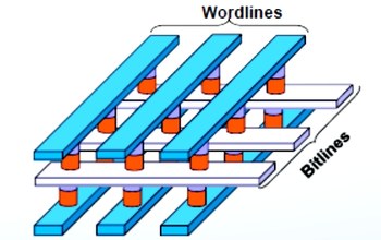
Non-conventional Memories
Scientific Coordinator: Prof. Massimo Rudan
In computer architectures, fast but small memories close to the processor are used as cache to have direct access to data. Large memories are mapped to the cache since they are slow for access to small data blocks but can provide large blocks of data in relatively little time. The gap between the two must be filled with non-volatile memories with large capacity (solid-state disk), whose latency and cost per bit are intermediate between those of the cache memory and the hard-disk drive. Among the new classes of non-volatile memories are phase-change memories (PCM) using chalcogenide alloys (e.g., GST-225). Energy (heat) converts material between crystalline (low resistance) and amorphous (high resistance) phases. They are extremely compact (unipolar selector), BEOL-compatible with the standard CMOS process, and allow for a True Cross Point Array (see figure). Other features are that PCM are stackable and easily scalable, and allow for a low-temperature process.
Main activities:
- Modeling transport in amorphous materials, including trap-to-trap and trap-to-band transitions, and time- and position-dependent temperature.
- Investigations on higher-order numerical schemes for solving the transport model.
Collaborations: UniMoRe, CNR IMM BO.
Research funded by Intel in the years 2007-2014.

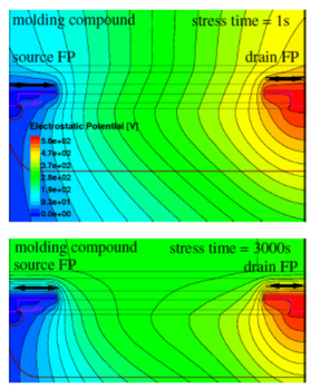
Characterization of the galvanic insulation of BCD processes and platforms
Scientific Coordinators: Prof. Andrea Cavallini, Prof. Davide Fabiani
The project will start September 2019. It aims at improving the galvanic insulation of power ICs based on the BCD (BIPOLAR-CMOS-DMOS) technology by
- an in depth-characterization of the polyimide and molding compound by measurements in DC (conductivity, space charge injection) and in AC (dielectric spectroscopy),
- the characterization of the processes leading to the formation of localized defects (delaminations, cavities, protrusions) supporting partial discharge activity.
These activities are carried on mainly within the joint STMicroelectronics-ARCES lab.